ELECTRONOTES
1016 Hanshaw Rd
Ithaca, NY 14850
(607)257-8010
Or you can visit the Electronotes web site at http://electronotes.netfirms.com/.
INTRODUCTION
There are six different VCO options for the ENS-76 system. Only option 1 will be shown here. If you are interested in the other options, you can order the original Electronotes issue EN#75 that contains details on all six options.
VCO OPTION 1: This VCO is pretty much a standard VCO, with the exception that it has a Linear FM input which had been added because it is useful and easy to implement. The basic oscillator was given by Terry Mikulic in EN#62 (13). This option is intended to give the greatest accuracy and range of any of the designs. We used a somewhat simpler exponential stage here. The heart of the design is really the Analog Devices type AD818 NPN matched pair which has been optimized by the manufacturer for log conformance. A small amount of reset compensation (R*) has been added to the design, but basically, we rely on the matched pair to keep the high end up (see the full circuit description for more information). The circuit has ± 10 volt signals throughout the waveshaping circuit, and it is trivial to bring out these signals, although we have chosen here to bring out our standard ±5 volt signals. We have used a "counter-glitch" correction in the saw-to-triangle converter (see the Utility VCO in EN#67), and becasue we have a ± 10 volt triangle available, it is convenient to use the FET type triangle-to-sine converter.
GENERAL FEATURES OF ALL THE OPTIONS
All the VCO's have the standard exponential response of 1 volt/octave with control voltages fed in through 100k. The output levels are ±5 volts, although it is generally possible to convert to a ± 10 volt system with little trouble. For the most part, signals are handled with the type 556 op-amp. In 5 volt systems, it is possible to use the 307 type op-amp if optimum high frequency preformance is not required.
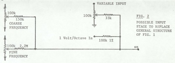
In order to simplify the schematic diagrams, we
have not shown specific input stages but instead will be using as an
input for control voltages the structure shown in Fig. 1.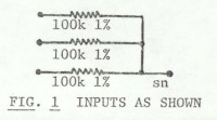 This could
of course be used as is, but we have in mind that in nearly all cases
the builder will use something with more features. In particular,
COARSE and FINE frequency controls are common, and variable input may
also be desired. There should be at least one input that is the
direct-in 100k 1% type. A possible input stage is shown in Fig. 2.
This could
of course be used as is, but we have in mind that in nearly all cases
the builder will use something with more features. In particular,
COARSE and FINE frequency controls are common, and variable input may
also be desired. There should be at least one input that is the
direct-in 100k 1% type. A possible input stage is shown in Fig. 2.
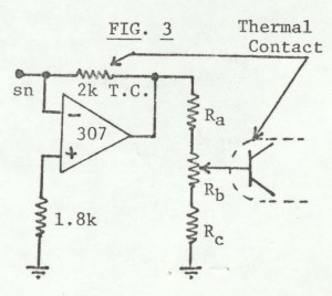
In practice, thermal contact is made by mounting the resistor and the transistor pair or array so that they are touching, and then putting a small amount of heat-sink compound between them. For set-up purposes and testing, an ordinary 2k 5% resistor can be used. The T.C. resistor and heat sink compound can be put in during final packaging and calibration.
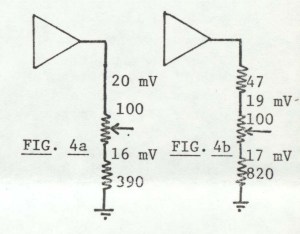
The resistors Ra, Rb (a trim pot, probably a multi-turn unit), and Rc are selected so that a one volt change at the input, through 100k, is scaled to an 18mV change at the wiper of the trim pot. At the same time, it is best to maintain a low source impedance (say 1k or lower) so that the base of the converting transistor is held down well. Since the output of the op-amp will never exceed a voltage of much more than a few hundred mV, there is no problem with the op-amp driving such a low impedance. In the circuit diagrams, we will be showing the voltage divider shown in Fig. 4a (Ra = 0, Rb = 100, Rc = 390) which permits the voltage to be scaled from any values between 20mV and 16mV. This works quite well if a multi-turn pot is used, and gives a lot of excess room on the ends. A somewhat tighter divider is shown in Fig. 4b, where Ra = 47, Rb = 100, and Rc = 820. This gives voltages scaled from 17 mV to 19mV. If you are using the precision resistors indicated (the 100k 1% or better), this should work out well. If however you are just setting up with 5% resistors, you may need the extra room given by the circuit of Fig. 4a.
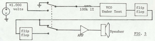
In any case, you will be adjusting the trim pot so that a 1 volt change at the input gives a one octave change of frequency. This should be set first at the lower frequencies (around 100 Hz) and then checked at higher frequencies, and compensated if necessary. Tuning is often best done by ear. As an aid, it is useful to have a precision one volt source which is switched in, and at the same time, a flip-flop is switched into the return line from the VCO. Thus, the pitch of the VCO should go up one octave, but the pitch returning should remain the same, because of the additional flip-flop. The original flip-flop is needed so that only square waves are compared. See Fig. 5 for this setup.
Most of the other adjustments and calibrations that you will need to make are described in the circuit descriptions of the various options. Keep in mind that there are six different circuits, and we built each one only once. If you copy ours exactly, it should work, but you may have to do a little trimmimg to get everything exactly the way you want it. We were not overly careful to adjust the amplitudes to exactly the five volt levels, and made no trim adjustment provisions for amplitude except in one case. You should trim these up if you find it necessary. You can use a scope to do this if you have an accurate one. However, even if you don't have an accurate scope, you can use an accurate meter. You just have to set the VCO frequency to 1/10 Hz or below and read the peak of the meter. For making adjustments of waveshapers, it is best to use a scope, even if it is a relatively poor one. Note however, that when trimming up the sine wave, the best instrument you have is your ear.
ENS-76 VCO OPTION 1The design goal for VCO Option 1 was to make a VCO with standard features that is as accurate and drift free as possible. The basic oscillator (IC-2 and IC-4) is a sawtooth generator based on the VCO described by Terry Mikaulic in EN#62. This basic oscillator is driven by an exponential current source based upon the Analog Devices type AD818 matched NPN pair, which is probably the best exponential (log) transistor pair available. The output of the basic oscillator is a zero to +5 volt ramp (output pin 6 of IC-2). The rest of the circuit consists of waveshapers that are more or less standard, and provide Saw, Triangle, Square, Pulse, and Sine outputs, all with ± 5 volt levels. It is easy to convert this one to ± 10 volt levels if this is desired. The circuit also has inputs for Linear Frequency Modulation, and for standard Pulse Width Modulation.
The exponential current source (IC-1, IC-3, T1 & T2) is a standard design which we have used many times before. Here we have improved things as much as possible by using the CA3140 op-amp to regulate the reference current, and the AD818 pair as the converting transistors. No provisions are made here for high end compensation of the exponential stage, but standard temperature compensation is made.
The basic oscillator is a sawtooth (ramp) relaxation oscillator formed from IC-2 and IC-4, and is only slightly changed from the original Mikulic design. IC-2 forms an integrator where the exponential current from the collector of T2 causes capacitor C1 to charge. For the moment, assume that R* is zero ohms. When the output of IC-2 reaches +5, the voltage on pin 2 of IC-4 is the same as the reference on pin 3 (as determined by voltage divider R13-Rl4), and as the voltage starts to rise above +5, comparator IC-4 goes from -15 to ground (pulled up by R15). This turns on the FET switch T3, and capacitor Cl begins to discharge rapidly. In general, the capacitor would discharge a little below +5 and the comparator would then shut off the FET switch. This would result in an output consisting of a high frequency oscillation of low amplitude centered about +5. This is where the capacitor C4 comes in. When the comparator switches high (to ground that is), the capacitor voltage is +20 volts (-15 from the comparator, and +5 fed in from the ramp through R12). This will cause to comparator to remain high until C4 discharges to +5 volts (starting at +20 and being discharged through.Rl2 to pin 6 of IC-2, which is going from +5 to zero). The time constant is thus something like 1.4 x Rl2 x C4, which is something like 400 ns. This is the time interval during which the FET switch will be on. This is long enough to completely discharge the capacitor for all practical purposes. Note finally that the discharge can be initiated a little early by the Sync. control input. A negative going pulse here will lower the reference a bit and institute the reset cycle.
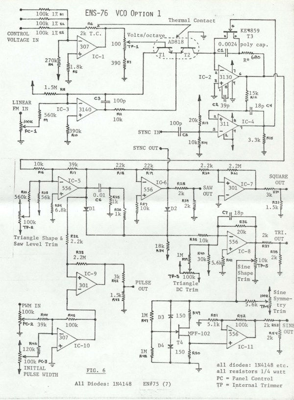
Rectangular waveforms are provided using uncompensated 301 type op-amps (or 748 types can be used). The square is provided by IC-7, and a variable pulse is provided by IC-9, relative to a reference voltage level provided by IC-10. This is all very standard, but keep in mind that both IC-7 and IC-9 are left completely uncompensated so that they will go as fast as possible (no capacitor between pins 1 and 8), and the positive feedback provided by the 2.2M resistors relative to the 2.2k input provides mild hysteresis for additional "snap" and noise rejection. The outputs of IC-7 and IC-9 range from +15 to -15, so 3k-1.5k voltage dividers are used to scale these to ±5 volt levels.
Finally, we use the FET type sinewave shaper as,driven by the triangle waveform. We chose this rather than the CA3080 shaper (used in later options) because it gives a slightly better looking waveform, and because we do have the ±10 volt triangle to drive it. It normally requires a 6 to 7 volt signal to reach the non-linear region.
It is probably obvious that since we are using ±10 volt
levels inside the circuit, it is easy to bring these out, For easy
reference, the conversion is listed below:
| RESISTOR | AS IS ±5 | CONVERSION TO ±10 |
| R28 | 2k | lk |
| R29 | 2k | Omit |
| R30 | 3k | 1.5k |
| R31 | 1.5k | 3k |
| R37 | 2k | lk |
| R38 | 2k | omit |
| R42 | 3k | 1.5k |
| R43 | 1.5k | 3k |
| R53 | 2k | lk |
| R54 | 2k | Omit |
At this point, we want to say something about the resistor
R*, which is the resistor that provides high frequency compensation by
Franco's method [See S. Franco, "Hardware Design of a Real-Time Musical
System", Dept of Computer Science Report UIUCDCS-R-74-677, Univ. of
Illinois, Urbana-Champaign]. The principle is basically as follows:
There is a finite switching time which causes an oscillator to go flat
on the high end. The higher frequencies correspond to higher charging
currents. Thus, by inserting a resistor in series with the integrating
capacitor, an additional voltage is impressed across the R-C
combination, and this causes the oscillator to reach its peak voltage a
little earlier. A full analysis (see reference above or chapter on
VCO's in MEH) will show that this is an exact correction for a constant
reset time, and that the R* x Cl product should be equal to the
switching time, which we saw above was about 400 ns. This gives a value
of R* of about 166 ohms. This is a good starting value. In addition, it
turns out that the error due to the bulk base-emitter resistance of the
exponential current stage transistors can be corrected by a term that
is the same order as the delay time correction. Thus, by making R*
larger than is necessary to correct for delay time, we can also do some
correction for bulk resistance. Of course, all the analysis in the
world is generally no substitute for an actual experiment, and we can
easily find the value for R* by an experiment - basically as shown in
Fig. 5.
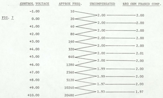
The data from an actual experiment is shown in Fig. 7.
It should not be too difficult to construct this circuit. A
little care should be used handling the MOS op-amps (CA3130 and
CA3140), and of course be careful with the expensive AD818 pair. All
op-amps are powered between +15 and -15 except for IC-2, the CA3130.
Also, be sure to note the unusual pin connections for the LM311
comparator, and be sure not to forget the pull-up resistor R15. All the
type 4859 FET's we have seen have the base diagram shown in Fig. 8, as
seen from the bottom view. 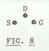
This includes the 2N4859, the KE4859, and the PN4859. Some may have three in-line wires at the very base, but will have the triangular diagram further out.
VIEW FROM 2001
One of the things about our Electronotes circuits and presentations, as opposed to the more usual "How to Build" publications, was that we always assumed our readers were knowledgeable, flexible, and willing to experiment. Indeed, it was the readers who provided most of the ideas for modifying and improving circuits. We expected different individuals to do things in different ways. In total, our presentations perhaps resembled musical compositions where we showed the official score, but at the same time, we encouraged different variations and interpretations of the score. This resulted in many interesting individual features and improvements. Looking back from 2001, when certain parts are difficult to obtain, and where fewer and fewer persons can offer useful help, the need to fully understand the circuit operation, and to understand parts substitutions, is of paramount importance.
Despite our encouragement of experimentation, one should not assume that arbitrary substitutions and modifications will not at times result in a substantially degraded performance. In regard to the Option 1 VCO, we note that there are three parts: the exponential converter, the sawtooth relaxation oscillator, and the waveshapers.
The exponential converter relied on the AD818 matched pair, which is probably hard to obtain today. This component was "brute force" and worth every penny. If you can't locate this, you really should go back to Terry Mikulic's original CA3046 array based converter. Do not assume that two unmatched transistors, even hand-matched and glued together, will be acceptable in terms of accuracy and stability.
The relaxation oscillator is Terry's original with a few modifications. As a general rule, for the entire circuit, you should be able to substitute LF351's or similar for the 556 , 301, and 307 op-amps. You can also use an LF351 for the CA3140. You can also use an LF351 for the CA3130, but it would be run on the bipolar supply, and without the 39p compensating capacitor. But keep the 311 comparator. The right FET could be very important. We only had success with the KE4859. Probably lots of other FETs would work, but of the very few more commonly available ones we tried, the sharp reset was missing.
The waveshapers are not too critical. If you are showing off the waveshapes with an oscilloscope, you might want them to look nice. But it is generally true, that for musical purposes, there is no requirement of even using this particular set of waveforms, let along a need to have these waveshapes without small imperfections.
As mentioned, there are many variations on this circuit which have appeared in various places. Here are two you should be aware of:
- Terry Michaels, "Modification to a VCO Design from 1976," Electronotes, Vol. 20, No. 194, April 2000
- http://ijfritz.byethost4.com/sy_cir2.htm This is from Ian Fritz, one of our major contributors from the "good old days."
Bernie Hutchins, April 2001
For more information, contact Electronotes at:
http://electronotes.netfirms.com/
ELECTRONOTES
1016 Hanshaw Rd
Ithaca, NY 14850
(607)257-8010